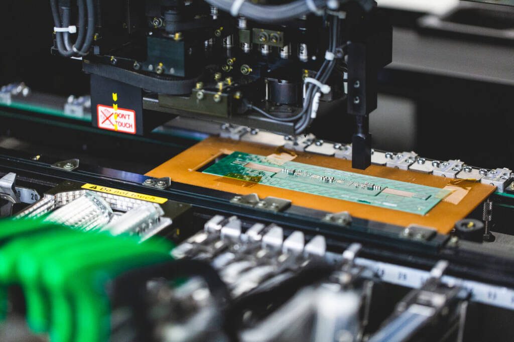
PCB Fabrication & Assembly (PCBA)
Fabricate, assemble, test, and ship—end‑to‑end production with rigorous quality checks and clear documentation.
From Gerbers to Box‑Ready Boards
We run DFM, fabricate with the right stackup and finish, assemble SMT/TH parts, inspect with AOI/X‑ray, validate with functional tests, and deliver ESD‑safe packed units—ready for pilot or production.

What You Get
Turnkey or consigned—our PCBA flow minimizes surprises and accelerates first‑pass yield.
DFM & Panelization
Gerber sanity checks, stackup selection, impedance targets, panel frames, fiducials, tooling holes, V‑cut/tab‑routing.
Fabrication
2 layers FR‑4 (Std/Hi‑TG), 1–3 oz Cu, ENIG/HASL‑LF/OSP, solder mask colors, tented vias, controlled impedance on request.
Assembly
Stencil + reflow (SMT), wave/selective (TH), fine‑pitch/QFN/BGA/uBGA, conformal coating optional, rework stations.
Inspection & Test
SPI/AOI, X‑ray for BGA, flying‑probe/ICT where applicable, functional test (FCT) jigs, burn‑in profiles for power boards.
Procurement & Alternates
Turnkey sourcing via Robu.in/Mouser India/element14/LCSC with vetted alternates; MSL handling & bake logs maintained.
Quality & Compliance
IPC‑A‑610 Class II/III, RoHS lead‑free, ESD‑safe packaging, traceability labels, and shipment QC reports.
How We Work
DFM Review & Quote
Review Gerbers/BOM/CPL, confirm stackup/finish, suggest risk fixes, finalize pricing and schedule.
Fabrication & Sourcing
Start fab and component procurement; create stencil and program PnP with reference designators.
Assembly & Inspection
SMT/TH assembly, reflow/wave, SPI/AOI/X‑ray checks, visual QA, and rework if needed.
Test, Pack & Ship
Run FCT/ICT/burn‑in as scoped, label units, ESD‑pack, share QC report and tracking. Pan‑India delivery.
Deliverables
- Assembled boards (PCBA) with serial/lot labels and COQ report
- QC pack: SPI/AOI/X‑ray images, reflow profile, test logs
- Packaging list + BoM revision + alternates actually used
- Leftover components, stencils, and programming files on request
